August 2016

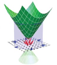
Tuning the valley and chiral quantum state of Dirac electrons in van der Waals heterostructures
Injecting electrons into one-atom-thick material graphene can control their movement, potentially leading to novel electronic applications, University of Manchester researchers have found.
Among the unusual properties of graphene, one of the most exciting and least understood is the additional degree of freedom experienced by electrons.
It is called the pseudospin and it determines the probability to find electrons on neighbouring carbon atoms. The possibility to control this degree of freedom would allow for new types of experiments, but potentially also enable to use it for electronic applications.
Now, writing in Science, Manchester physicists demonstrate how electrons with well-controlled pseudospin can be injected into graphene. The scientists used two layers of graphene, rotated by a small angle with respect to each other and separated by a thin layer of boron nitride, another two-dimensional material and an excellent insulator.
Applying strong magnetic field parallel to the graphene layers, the pseudospin state of the tunnelling electrons can be chosen.
Tuning the valley and chiral quantum state of Dirac electrons in van der Waals heterostructures, by J. R. Wallbank, D. Ghazaryan, A. Misra, Y. Cao, J. S. Tu, B. A. Piot, M. Potemski, S. Pezzini, S. Wiedmann, U. Zeitler, T. L. M. Lane, S. V. Morozov, M. T. Greenaway, L. Eaves, A. K. Geim, V. I. Fal'ko, K. S. Novoselov, A. Mishchenko
March 2016
Macroscopic self-reorientation of interacting two-dimensional crystals
Precise control of motion in microelectromechanical systems can be invaluable to advanced technologies.
Here, a team Led by Prof. Novoselov, demonstrate that such accuracy can be achieved in two-dimensional crystals interacting through the van der Waals forces. Self-reorientation has been shown to take place for the situation of graphene on hexagonal Boron Nitride with macroscopic movement of hundreds of nanometres.
The underlying mechanism also has clear extensions to many other similar 2D crystals.
January 2016
High thermal conductivity of hexagonal boron nitride laminates
The hexagonal Boron Nitride, the electrically insulating counterpart of graphene, can potentially become the game-changer in thermal management.
Rapid miniaturization of modern electronics puts demand for ever more efficient heat removal and dissipation. One of the main difficulties faced by the industry is the realization of highly efficient electrically insulating heat spreaders and novel materials for thermally conductive PCBs. In this respect hexagonal Boron Nitride is the most promising material which combines excellent dielectric properties with high thermal conductivity and potentially low production costs.
Our group led by Prof. Kostya Novoselov in collaboration with the group of Prof. Miao Lu from Xiamen University and BGT Materials Limited developed and characterised a novel thermally conductive laminate film produced from hexagonal Boron Nitride inks. This laminate film can be used as conformal coatings or free-standing membranes with the in-plain thermal conductivity which matches that of alumina, and can be tuned by changing the laminate density. Being electrically insulating, hBN laminates can potentially overcome many of the problems associated with electrically conductive materials and open a new era in advanced thermal management materials. The results of this work have been published in the latest issue of 2D Materials.
January 2016
Gain modulation by graphene plasmons in aperiodic lattice lasers
Research carried out by a team of researchers, led by Dr Subhasish Chakraborty and Sir Kostya Novoselov, reported in journal Science, that graphene could be used to control the frequency of terahertz lasers.
Terahertz technology exists on the electromagnetic spectrum between microwave and infrared frequencies. The benefit of using terahertz lasers instead of X-rays is that they can accurately scan materials without causing damage. Highly-sensitive scanners for sensing minute defects in manufactured drugs, or detecting concealed weapons at airports could become more accurate and much safer for frequent use using the new technology.
Terahertz lasers are similar to X-rays in that they are invisible to the naked eye but are far safer in comparison by being non-destructive and non-invasive. The research could vastly improve scanning systems, replacing X-rays, and also dramatically increase internet bandwidth, and could dramatically improve the efficiency and accuracy of analysing materials in the pharmaceutical, security and agricultural industries.
Dr Chakraborty said: “Terahertz technologies have been somewhat ignored by industry, partly due to the complexity of creating high-power tunable devices, as lots of different materials were necessary.
“Graphene can now fill in the gaps of this technology by creating a platform to electronically control devices and flexibly engineer device output”.
Sir Kostya said: “Current terahertz devices do not allow for tuneable properties, a new device would have to be made each time requirements changed, making them unattractive on an industrial scale.
“Graphene however, can allow for terahertz devices to be switched on and off, as well as altering their state.”
The introduction of tuneable properties thanks to graphene could also potentially increase internet bandwidth capabilities up to and beyond one terabyte per second, a vast improvement on current internet speeds.
The full story on the University of Manchester website can be found here.
November 2015
Resonant tunnelling between the chiral Landau states of twisted graphene lattices
Research collaboration between the Universities of Manchester, Nottingham, Lancaster and colleagues at Institute of Microelectronics Technology and High Purity Materials, National University of Science and Technology ‘MISiS’ in Russue, may lead to a new area of electronics.
Graphene is a single layer of carbon atoms held together by strong covalent bonds, with 3 bonds linking each atom to its nearest neighbours, a periodic array of hexagonal unit cells. Each carbon atom provides 6 electrons and each bond is made up of 2 electrons, but some of the electrons can move freely and when we apply a voltage to the graphene, an electrical current flows along the graphene layer.
In ordinary metals and semiconductors, the electrons have a mass which has a slightly different value from that of an electron moving in a vacuum but we can think of a free electron behaving like a pinball: the harder we push it, the faster it moves. In graphene, the electrons move and respond to electrical forces quite differently. No matter how hard the push, their speed remains the same even if they gain more energy, moving at a speed of a million metres per second.
Graphene’s electrons have another rather strange property, “chirality” that makes them different from electrons in ordinary solids. We investigate chirality by studying the way in which current flows in a simple sandwich structure in which a layer of graphene is placed on each side of a 4 atomic layer thick sheet of boron nitride. This barrier is thin enough to allow electrons to pass between the graphene layers by quantum tunnelling when we apply a voltage between the two layers.
To understand chirality, look down at your shoes or bare feet. The right one is different from the left one. When looking at the left foot in a mirror, its image looks like your real right foot. Electrons in graphene and the states that they occupy can be thought of as either “right-footed” or “left-footed” and the states that they can occupy are like shoes, either filled, or empty of electrons. Like shoes, the states can either be filled or empty, with the correctly-fitting electron. With no voltage applied, the electrons occupy a large and equal number of left- and right-footed states in each graphene sheet, and the total number of occupied states in each sheet is the same. The electric current due to electrons tunnelling through the boron nitride barrier is caused by electrons leaving the filled states of the negatively-charged graphene layer and moving into the empty states of the other. When tunnelling, the right-footed electrons much prefer to find right-footed states to fit into as there is a quantum mechanical ”selection rule” which prevents them fitting into the opposite.
The physical origin arises from the symmetry of the “chicken wire” graphene lattice. Half of the atoms have one symmetry - one group of atoms having a horizontal bond pointing to the left and two angled bonds pointing to the right, the other a mirror image of this arrangement. This, combined with the relativistic behaviour of the massless electrons in graphene, is the origin of the “right-footed” and “left-footed” shoe analogy.
Electronics, which is a technology for processing information by controlling the free motion of electrons, revolutionised technology in the twentieth century; spintronics is currently being studied with a view to using the spin of electrons for storing and transmitting information. It will be interesting to see if the chirality of electrons in graphene-based electronic devices can be exploited to develop a new technology – “chiraltronics”.
10.1038/ncomms9846
November 2015
Graphene plasmonics illuminates a new logic
Wonder material graphene has been utilised to produce an optical modulator for a nascent optical micro-circuitry technology, thanks to research carried out by University of Manchester scientists.
Presenting their work in Nature Communications, the team, comprising of a collaboration between the Universities of Manchester and South Denmark, fabricated the modulator devices on top of plasmonic waveguides using graphene and its sister two-dimensional material boron nitride.
Plasmonics is the study of the collective oscillations of electrons generally on the surface of materials. Excitations based on this phenomenon, known as plasmons, are able to flow, and much research is ongoing worldwide to develop components that would allow these plasmons to be controlled in much the same way as electrons are controlled in electronic circuitry. The development of an efficient modulator that can switch on and off the flow of plasmons at fast speeds is therefore of critical importance.
Due to the unique optical and electronic properties of graphene, the team, led by Prof Sasha Grigorenko, were able to control how much electromagnetic energy the graphene layer in the modulator device could absorb, by applying an external voltage. As flowing plasmons generate an electric field (and associated electromagnetic energy), this tuning of absorptivity caused a modulation of the plasmonic signal at the end of the waveguide, as a varying amount of the energy was being lost to the graphene layer. The device size was 10 um^2 - about the surface of a single human red blood cell.
Hybrid graphene modulators offer great switching speeds, low power consumption and small physical footprints, critical figures of merit in telecommunications and optoelectronics. By utilising the capability of plasmonic devices to be produced at sizes below the wavelength of light - a stumbling block for the development of analagous integrated optical technologies - it is expected that further miniaturisation should be possible.
The scientists, from the School of Physics and Astronomy, hope that the research can help pave the way to the future realisation of all-plasmonic, on-chip circuitry.
10.1038/ncomms9846
July 2015
High Broad-Band Photoresponsivity of Mechanically Formed InSe–Graphene van der Waals Heterostructures
The isolation of single layer graphene has increased interest in other 2D crystals – particularly those with strong in plane bonds and weaker interlayer couplings. Layering these crystals, we can create devices and the electronic properties of these can be altered by careful selection of the materials within the stack as well as adjusting the built-in strain and relative orientation of the component crystalline layers.
Among the van der Waals crystals, the metal chalcogenide III–VI compound, InSe, represents an exfoliable and stable semiconductor that extends the library of vdW crystals.
Research undertaken in collaboration between the University of Manchester and the University of Nottingham, has determined the high broad-band photoresponsivity of mechanically formed InSe–graphene van der Waals heterostructures is achieved by exploiting the broad-band transparency of graphene, the direct bandgap of InSe, and the favorable band line up of InSe with graphene. The result is photoresponsivity that exceeds that present in other van der Waals heterostructures and spectral response that extends from the near-infrared to the visible spectrum.
The heterostructure of graphene and InSe is a good photodetector because of efficient charge carrier extraction at the graphene-InSe interfaces due to a low potential barrier. As graphene is so transparent, it means there is very high transmission of light into the InSe through the top graphene electrode, which is desirable in a photodetector. This will in time result in the ability to build more responsive photodetectors from vdW heterostructures due to the properties of the graphene electrode interface to the active material.
June 2015
Graphene-hBN resonant tunneling diodes as high-frequency oscillators
Collaboration between the University of Manchester and the University of Nottingham into the possibility of utilising two-terminal graphene-hBN-graphene resonant tunneling diodes as high-frequency oscillators has indicated that devices operational at several hundred GHz should be achievable.
Using self-consistent quantum transport and electrostatic simulations, researchers determined the time-dependent response of the diodes in a resonant circuit and quantified how the frequency and power of the current oscillations depend on the diode and circuit parameters, doping of the graphene electrodes, device geometry and alignment of the graphene lattices. This research illustrates further potential for the world of graphene electronics
May 2015
Exciton-polaritons in van der Waals heterostructures embedded in tunable microcavities
In collaboration with the University of Sheffield, research on vertically assembled layered van der Waals (VDW) heterostructures has resulted in a pathway for the observation of exciton-polaritons in 2D semiconducting crystals.
The isolation of single layer graphene has led to the rapid exploration of new 2D crystals with a variety of different properties
This research takes advantage of the high optical quality of single layer molybdenum diselenide (MoSe2 – a direct band gap semiconductor) on hexagonal boron nitride (hBN) substrates. By embedding multiple MoSe2/hBN stacks within an optical microcavity and exciting with a laser, it causes the emitted light (photoluminescence) to strongly couple with the optically excited charge carriers (electrons and holes which together form excitons). This leads to the creation of half-light/half-matter quantum states called exciton-polaritons. This work shows that by increasing the number of quantum wells by adding extra hBN and MoSe2 it is possible to increase the coupling strength which may allow for room temperature operation.
This work is the first step towards the creation of low threshold polariton lasers based on transition metal dichalcogenides, which can operate at room temperature.
December 2014
Protons go through one-atom-thick crystals
Graphene, impermeable to all gases and liquids, can easily allow protons to pass through it, as reported in Nature by Manchester researchers.
The group has tested whether protons are blocked by graphene and other 2D crystals, as predicted by theory. They found that protons pass through graphene surprisingly easily, especially at elevated temperatures and if the films were covered with catalytic nanoparticles such as platinum.
This finding makes monolayers of graphene, and its sister material boron nitride, attractive for possible uses as proton-conducting membranes, which are at the heart of modern fuel cell technology.
“Proton transport through one-atom-thick crystals” 10.1038/nature14015.
October 2014
Valley currents in graphene superlattices
In graphene superlattices, electrons move at a controllable angle to applied fields, similar to sailboats driven diagonally to the wind, as reported in Science by Manchester researchers.
In original graphene, charge carriers behave like massless neutrinos moving at the speed of light and having the electron charge. Electrons in graphene superlattices are different and behave as neutrinos that acquired a notable mass. This results in a new, relativistic behaviour so that electrons can now skew at large angles to applied fields. The effect is huge.
“Topological currents in graphene superlattices” 10.1126/science.1254966.
September 2014
Impermeable barrier films and protective coatings based on reduced graphene oxide

A thin layer of graphene paint can make impermeable and chemically resistant coatings which could be used for packaging to keep food fresh for longer and protect metal structures against corrosion, new findings from The University of Manchester show.
The surface of graphene, a one atom thick sheet of carbon, can be randomly decorated with oxygen to create graphene oxide; a form of graphene that could have a significant impact on the chemical, pharmaceutical and electronic industries. Applied as paint, it could provide an ultra-strong, non-corrosive coating for a wide range of industrial applications.
Graphene oxide solutions can be used to paint various surfaces ranging from glass to metals to even conventional bricks. After a simple chemical treatment, the resulting coatings behave like graphite in terms of chemical and thermal stability but become mechanically nearly as tough as graphene, the strongest material known to man.
“Impermeable barrier films and protective coatings based on reduced graphene oxide” DOI:10.1038/ncomms5843
The full story on the University of Manchester website can be found here.
September 2014
Twist-controlled resonant tunnelling in graphene/boron nitride/graphene heterostructures
Electronc properties of graphene/ boron nitride/graphene tunnelling diodes depend crucially on the relative orientation of the graphene electrodes, as reported in Nature Nanotechnology by Manchester researchers.
Recent developments in the technology of van der Waals heterostructures made from two-dimensional atomic crystals have already led to the observation of new physical phenomena. An unprecedented degree of control of the electronic properties is available not only by means of the selection of materials in the stack, but also through the additional finetuning achievable by adjusting the built-in strain and relative orientation of the component layers. Here we demonstrate how careful alignment of the crystallographic orientation of two graphene electrodes separated by a layer of hexagonal boron nitride in a transistor device can achieve resonant tunnelling with conservation of electron energy, momentum and, potentially, chirality. We show how the resonance peak and negative differential conductance in the device characteristics induce a tunable radiofrequency oscillatory current that has potential for future high-frequency technology.
“Twist-controlled resonant tunnelling in graphene/boron nitride/graphene heterostructures” DOI:10.1038/nnano.2014.187
The full story on the University of Manchester website can be found here.
April 2014
Commensurate–incommensurate transition in graphene on hexagonal boron nitride
In this work, the graphene lattice is found to stretch locally to match the 1.8% larger hBN lattice (the commensurate state). This transformation only occurs when the angle between the two crystals is less than approximately 1 degree. Reported here are atomic force microscopy (AFM) experiments on the superlattice, with complimentary Raman spectroscopy, electronic transport, and scanning tunnelling microscopy experiments. The AFM data demonstrates abrupt changes in Young’s modulus across the superlattice period for aligned (1 degree) samples, which contrasts to the smooth variation in Young’s modulus for unaligned samples. This is indicative of the formation of commensurate domains separated by strain accumulating domain walls (described in one dimension by the Frenkel-Kontorova model), with the disappearance of the effect for unaligned samples associated with the increasing complexity of the Peierl’s potential. To confirm this interpretation, the relative lattice constant for graphene within the commensurate domains, as compared to the domain walls, was found to be 2% larger from atomic resolution scanning tunnelling microscopy. In the Raman spectrum of graphene, the width of the 2D peak is found to broaden as the alignment becomes better, which results from the increased strain distribution of the commensurate state. Furthermore, Electronic transport measurements exhibit an opening/increasing energy gap associated with the formation of the commensurate state, albeit small in size.
“Commensurate–incommensurate transition in graphene on hexagonal boron nitride” DOI:10.1038/nphys2954
The full story on the University of Manchester website can be found here.
June 2013
Controlling magnetic clouds in graphene
“Dual origin of defect magnetism in graphene and its reversible switching by molecular doping” DOI: 10.1038/ncomms3010
May 2013
Cloning of Dirac fermions in graphene superlattices
Here we report transport properties of graphene placed on a boron nitride substrate and accurately aligned along its crystallographic directions. The substrate’s moire´ potential acts as a superlattice and leads to profound changes in the graphene’s electronic spectrum. Secondgeneration Dirac points appear as pronounced peaks in resistivity, accompanied by reversal of the Hall effect. The latter indicates that the effective sign of the charge carriers changeswithin graphene’s conduction and valence bands. Strong magnetic fields lead to Zaktype cloning of the third generation of Dirac points, which are observed as numerous neutrality points in fieldswhere a unit fraction of the flux quantum pierces the superlattice unit cell. Graphene superlattices such as this one provide a way of studying the rich physics expected in incommensurable quantum systems and illustrate the possibility of controllably modifying the electronic spectra of two-dimensional atomic crystals by varying their crystallographic alignment within van derWaals heterostuctures.
The full story on the University of Manchester website can be found here.
May 2013
Heterostructures based on 2D atomic crystals for flexible photovoltaic applications
The development of graphene technology led to the discovery of the whole new family of one-atom-thick materials. Collectively, such materials cover an extremely large parameter space of properties: from the most conductive to insulating, from strongest to softest, from opaque to optically transparent, etc.
Recently, researchers came with a new paradigm in material science: heterostructures based on such 2D materials. Combining several of such one atom thick layers in a three-dimensional stuck, researchers have been able to observe extremely exciting physical phenomena and come with a range of new electronic devices. Furthermore, every new layer of 2D materials in such stack add new functionality, so this paradigm is very natural for creation of novel, multifunctional devices. It is exactly the case when one plus one is greater than two – the combinations of 2D crystals allows one to achieve functionality not available from any of the individual monolayers.
In this paper, researchers from Manchester and Singapore expanded the functionality of such heterostructures to optoelectronics and photonics. By combining graphene with monolayers of transition metal dichalcogenides (TMDC) the researchers were able to created extremely sensitive and efficient photovoltaic devices. Such devices could potentially be used as ultrasensitive photodetectors or very efficient solar cells. In these devices, layers of TMDC were sandwiched between two layers of graphene, combining the exciting properties of both 2D crystals. TMDC layers act as very efficient light absorbers and graphene as a transparent conductive layer. This will allow for further integration of such photovoltaic devices into more complex, more multifunctional heterostructures. DOI: 10.1126/science.1235547
The full story on the University of Manchester website can be found here.
April 2013
Graphene-based transistor with bistable characteristics
Writing in Nature Communications, researchers from Manchester and Nottingham report the first graphene-based transistor with bistable characteristics, which means that the device can spontaneously switch between two electronic states. Such devices are in great demand as emitters of electromagnetic waves in the high-frequency range between radar and infra-red, relevant for applications such as security systems and medical imaging.
Bistability is a common phenomenon – a seesaw-like system has two equivalent states and small perturbations can trigger spontaneous switching between them. The way in which charge-carrying electrons in graphene transistors move makes this switching incredibly fast – trillions of switches per second.
The device consists of two layers of graphene separated by an insulating layer of boron nitride just a few atomic layers thick. The electron clouds in each graphene layer can be tuned by applying a small voltage. This can induce the electrons into a state where they move spontaneously at high speed between the layers.
Because the insulating layer separating the two graphene sheets is ultra-thin, electrons are able to move through this barrier by ‘quantum tunnelling’. This process induces a rapid motion of electrical charge which can lead to the emission of high-frequency electromagnetic waves.
These new transistors exhibit the essential signature of a quantum seesaw, called negative differential conductance, whereby the same electrical current flows at two different applied voltages. The next step for researchers is to learn how to optimise the transistor as a detector and emitter.
The full story on the University of Manchester website can be found here.
February 2013
Interaction phenomena in graphene seen through quantum capacitance
Capacitance measurements provide a powerful means of probing the density of states. The technique has proved particularly successful in studying 2D electron systems, revealing a number of interesting many-body effects. Here, we use large-area high-quality graphene capacitors to study behaviour of the density of states in this material in zero and high magnetic fields. Clear renormalization of the linear spectrum due to electron–electron interactions is observed in zero field. Quantizing fields lead to splitting of the spin- and valley-degenerate Landau levels into quartets separated by interaction-enhanced energy gaps. These many-body states exhibit negative compressibility but the compressibility returns to positive in ultrahigh magnetic fields. The reentrant behaviour is attributed to a competition between field-enhanced interactions and nascent fractional states.
The full story on the University of Manchester website can be found here.
In a paper published in Science, a Manchester team lead by Professor Sir Andre Geim and Professor Sir Kostya Novoselov has literally opened a third dimension in graphene research. One of many potential applications of graphene is its use as the basic material for computer chips instead of silicon. This potential has alerted the attention of major chip manufactures, including IBM, Samsung, Texas Instruments and Intel to name but a few. Individual transistors with very high frequencies (up to 300 GHz) have already been demonstrated by several groups worldwide. Unfortunately, those transistors cannot be packed densely in a computer chip because they leak too much current, even in the most insulating state of graphene. This electric current would cause chips to melt within a fraction of a second.
The University of Manchester scientists now suggest using graphene not laterally (in plane) – as all the previous studies did – but in the vertical direction. Here graphene gets help from other one atom thick materials. Sandwiched together they acquire extra functionality. Particularly graphene can be used as an electrode from which electrons tunnelled through a dielectric into another metal. This is called a tunnelling diode.
Even better, such “Layer Cake” superstructure can be used as a transistor. Manchester scientists exploited a truly unique feature of graphene – that an external voltage can strongly change the energy of tunnelling electrons. As a result they got a new type of the device – vertical field-effect tunnelling transistor in which graphene is a critical ingredient.
Dr Leonid Ponomarenko, who spearheaded the experimental effort, said: “We have proved a conceptually new approach to graphene electronics. Our transistors already work pretty well. I believe they can be improved much further, scaled down to nanometre sizes and work at sub-THz frequencies.”
Graphene has revealed another of its extraordinary properties - University of Manchester researchers have found that it is superpermeable with respect to water.
Graphene is one of the wonders of the science world, with the potential to create foldaway mobile phones, wallpaper-thin lighting panels and the next generation of aircraft. The new finding at The University of Manchester gives graphene’s potential a most surprising dimension – graphene can also be used for distilling alcohol.
In a report published in Science, a team led by Professor Sir Andre Geim shows that graphene-based membranes are impermeable to all gases and liquids (vacuum-tight). However, water evaporates through them as quickly as if the membranes were not there at all.
Now the University of Manchester scientists have studied membranes from a chemical derivative of graphene called graphene oxide. Graphene oxide is the same graphene sheet but it is randomly covered with other molecules such as hydroxyl groups OH-. Graphene oxide sheets stack on top of each other and form a laminate.
The researchers prepared such laminates that were hundreds times thinner than a human hair but remained strong, flexible and were easy to handle.
When a metal container was sealed with such a film, even the most sensitive equipment was unable to detect air or any other gas, including helium, to leak through.
It came as a complete surprise that, when the researchers tried the same with ordinary water, they found that it evaporates without noticing the graphene seal. Water molecules diffused through the graphene-oxide membranes with such a great speed that the evaporation rate was the same independently whether the container was sealed or completely open.
Dr Rahul Nair, who was leading the experimental work, offers the following explanation: “Graphene oxide sheets arrange in such a way that between them there is room for exactly one layer of water molecules. They arrange themselves in one molecule thick sheets of ice which slide along the graphene surface with practically no friction.
“If another atom or molecule tries the same trick, it finds that graphene capillaries either shrink in low humidity or get clogged with water molecules.”
“Helium gas is hard to stop. It slowly leaks even through a millimetre -thick window glass but our ultra-thin films completely block it. At the same time, water evaporates through them unimpeded. Materials cannot behave any stranger,” comments Professor Geim. “You cannot help wondering what else graphene has in store for us”.
“This unique property can be used in situations where one needs to remove water from a mixture or a container, while keeping in all the other ingredients”, says Dr Irina Grigorieva who also participated in the research.
“Just for a laugh, we sealed a bottle of vodka with our membranes and found that the distilled solution became stronger and stronger with time. Neither of us drinks vodka but it was great fun to do the experiment”, adds Dr Nair.
The Manchester researchers report this experiment in their Science paper, too, but they say they do not envisage use of graphene in distilleries, nor offer any immediate ideas for applications.
However, Professor Geim adds ‘The properties are so unusual that it is hard to imagine that they cannot find some use in the design of filtration, separation or barrier membranes and for selective removal of water’.