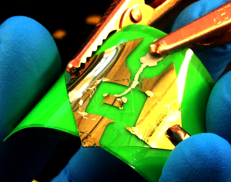
To illustrate our results
Some selective images that we like
Click on the picture to get a higher resolution image

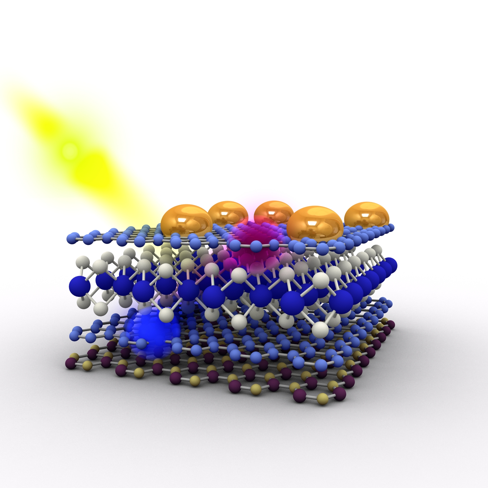
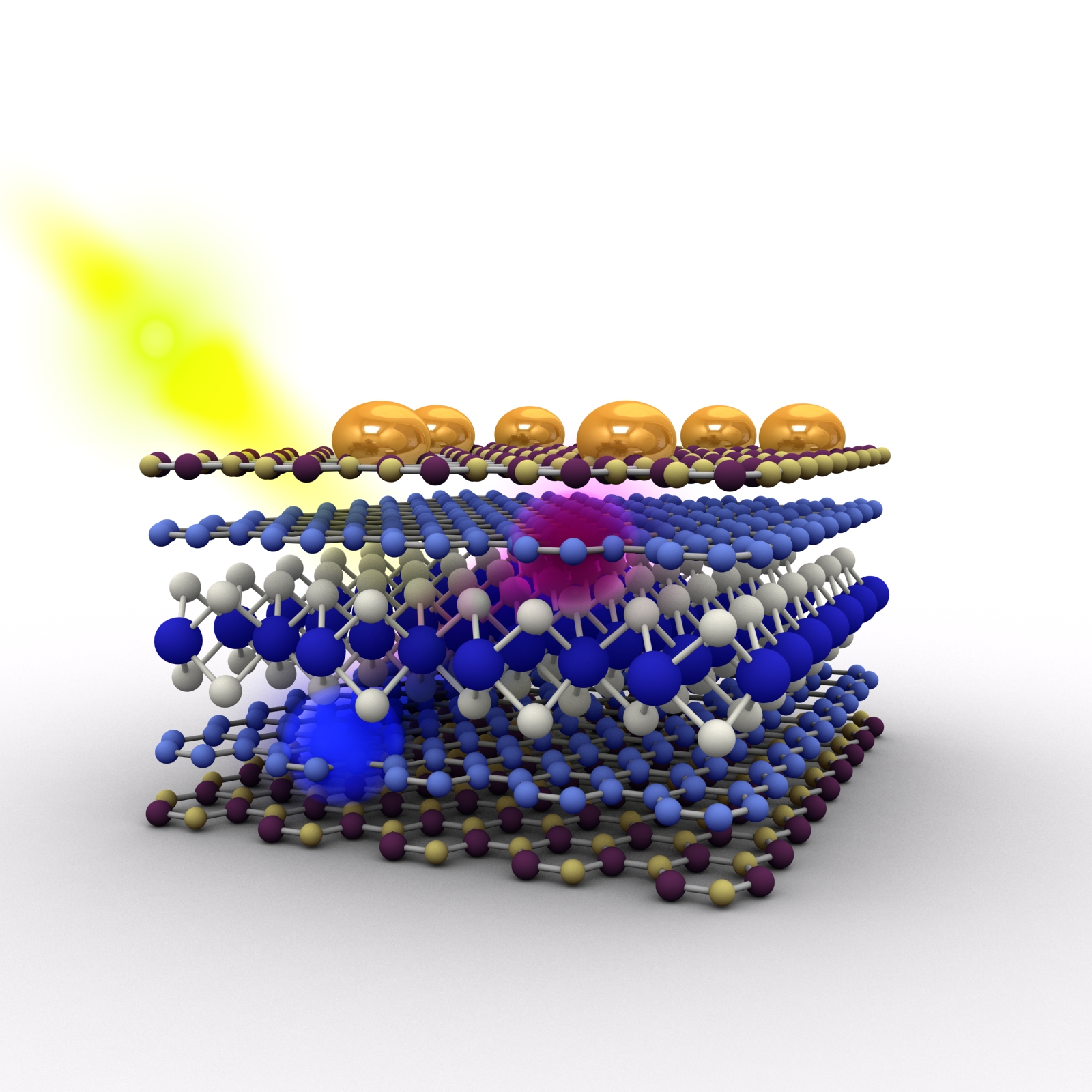
Tuning the valley and chiral quantum state of Dirac electrons in van der Waals heterostructures
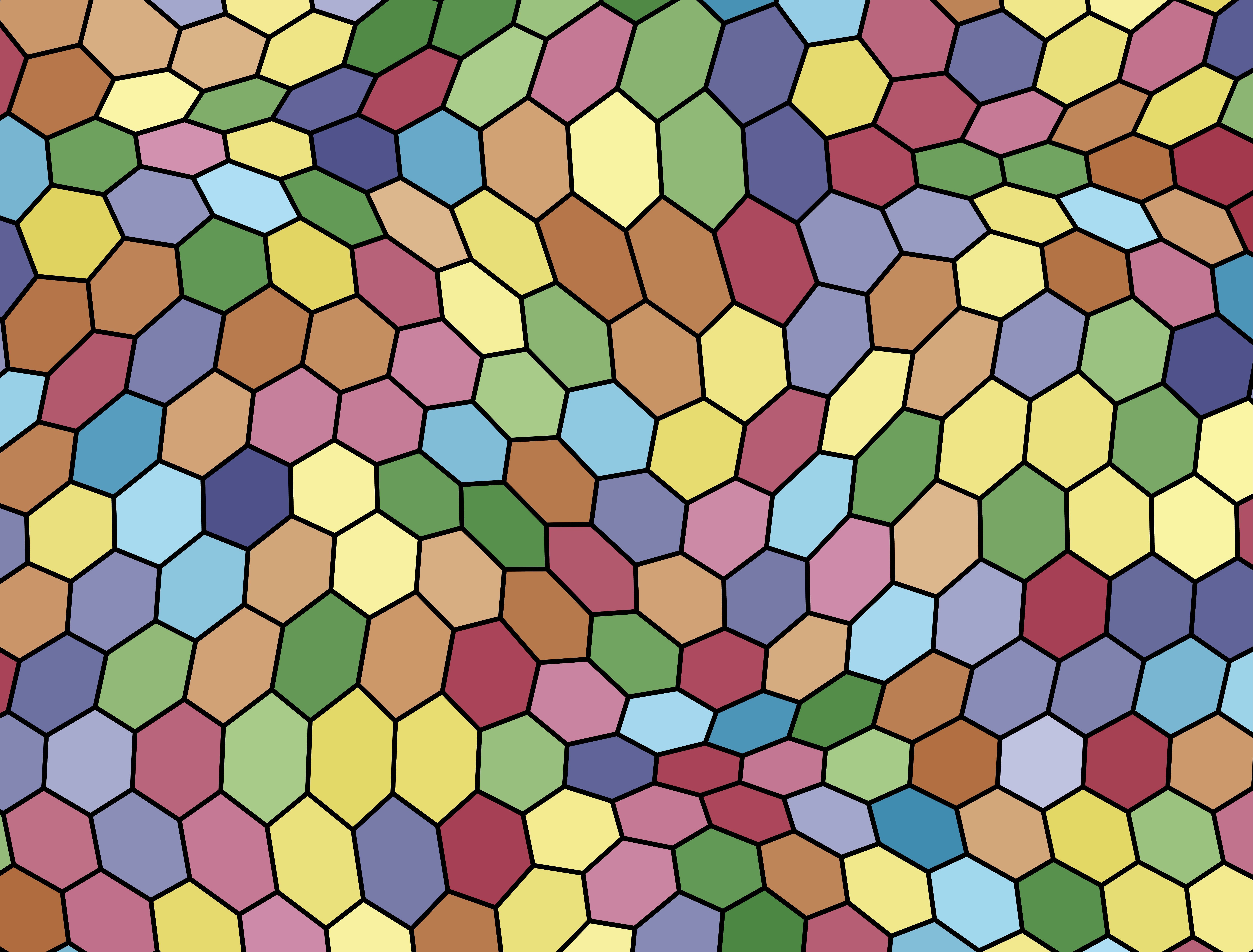
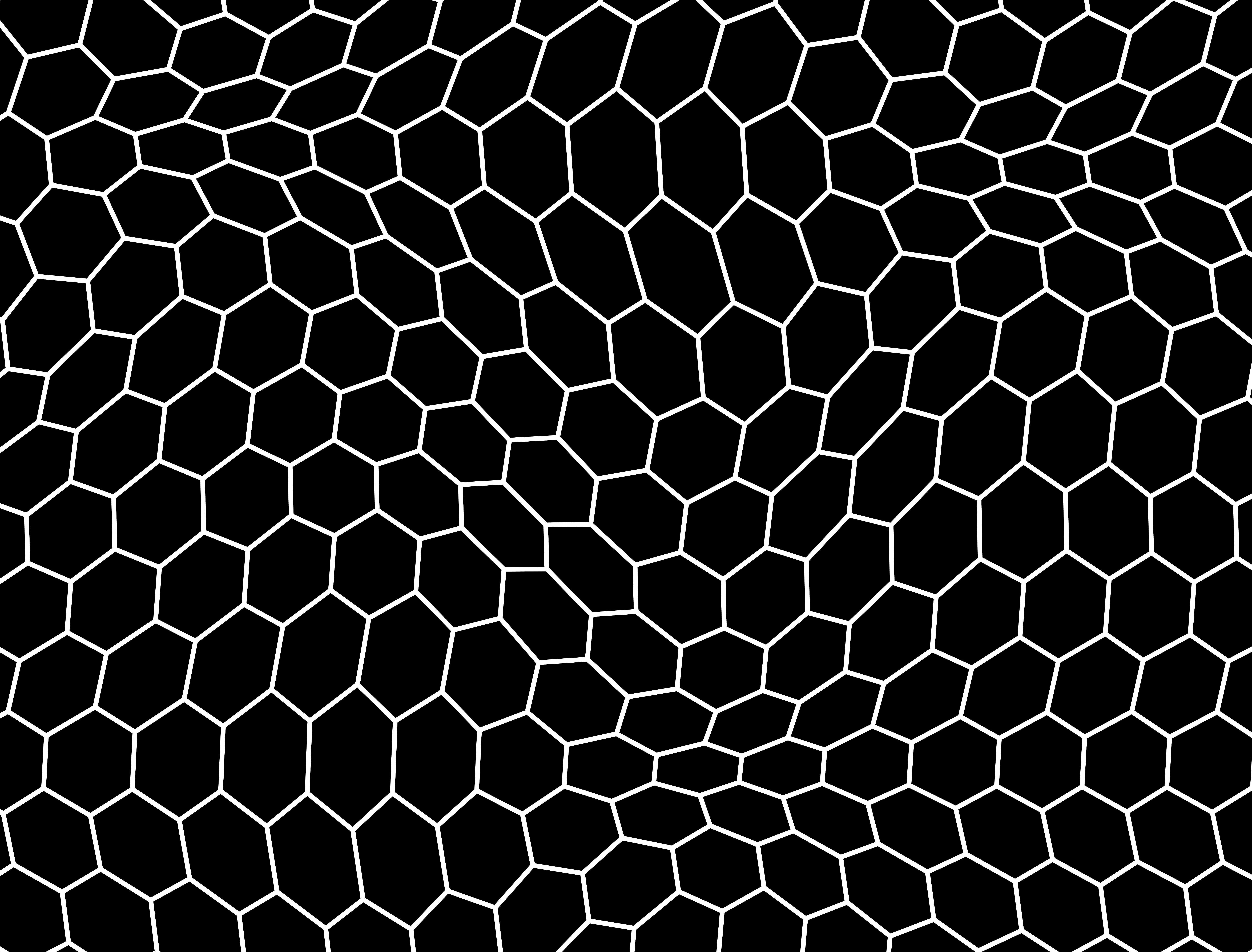
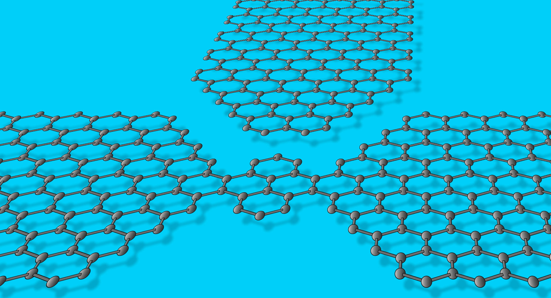
Moire pattern for graphene on hexagonal boron nitride.
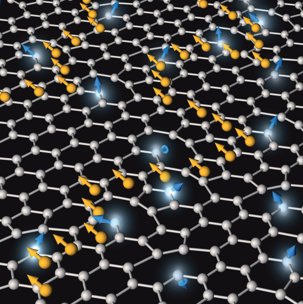
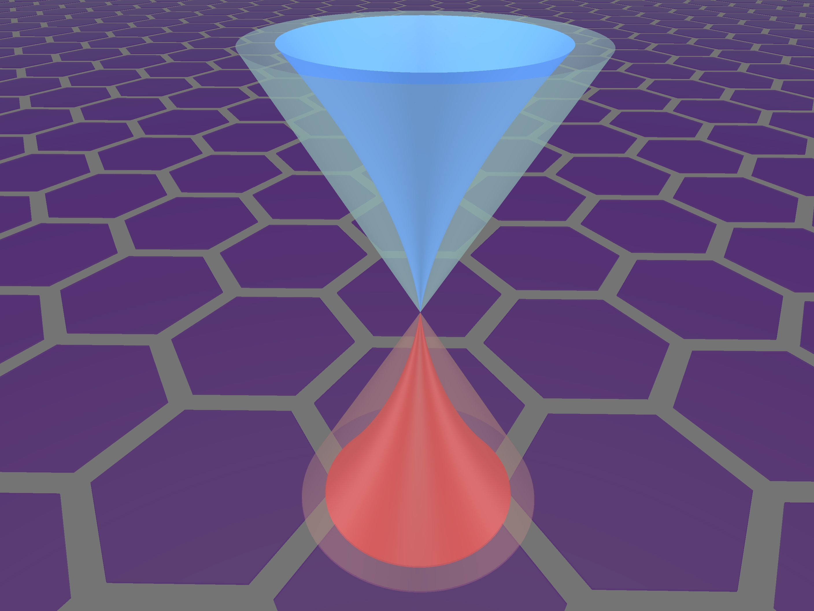
Controlling magnetic clouds in graphene.
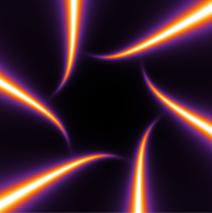
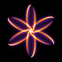
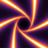
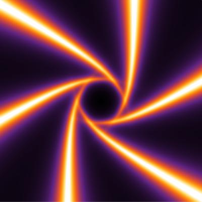
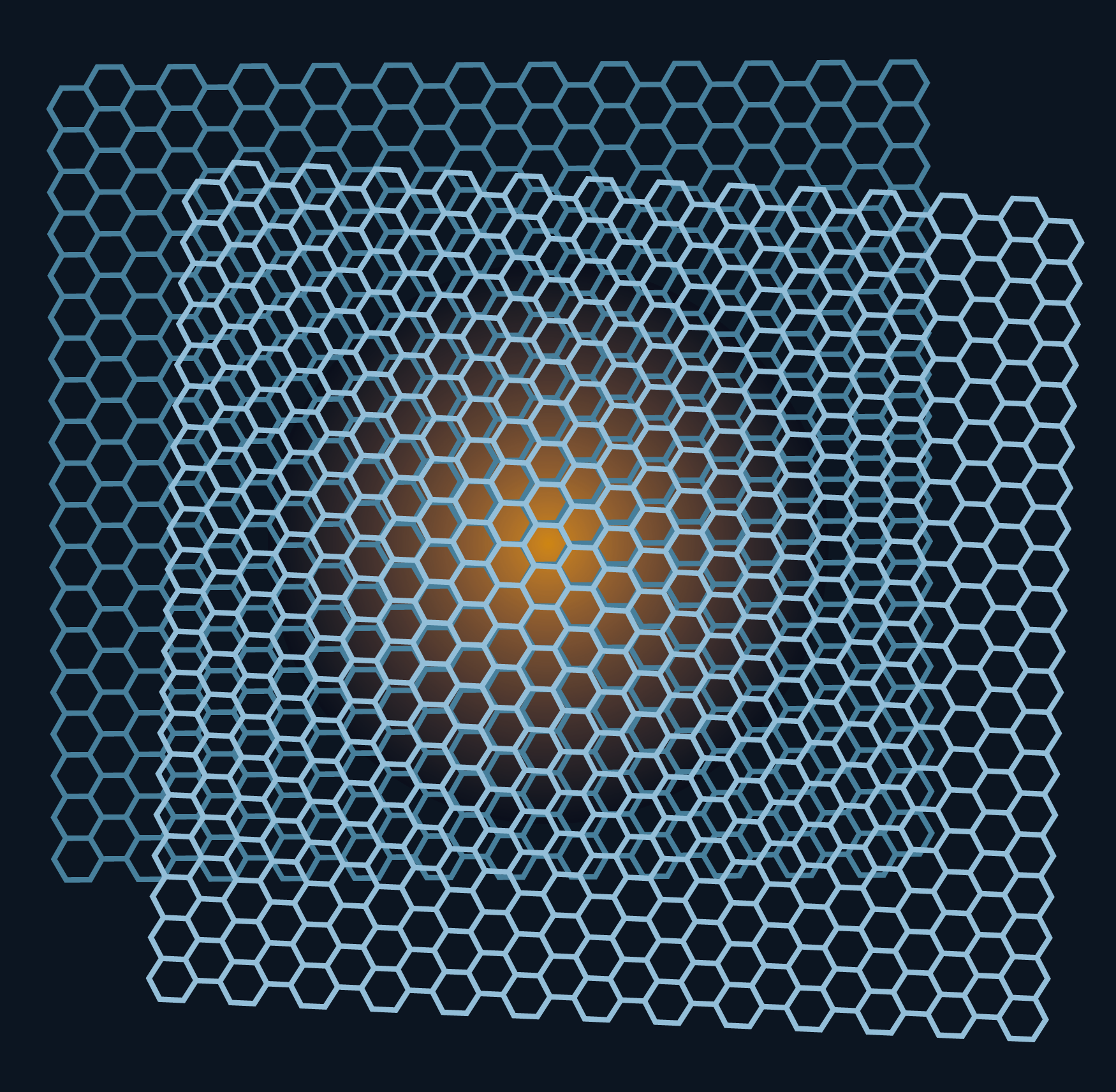
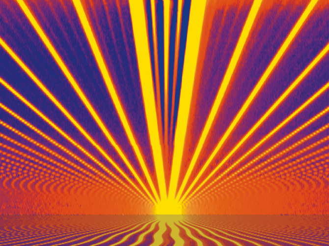
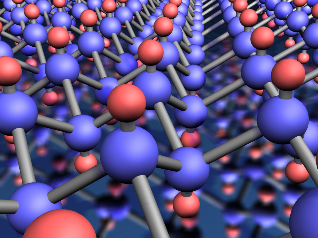
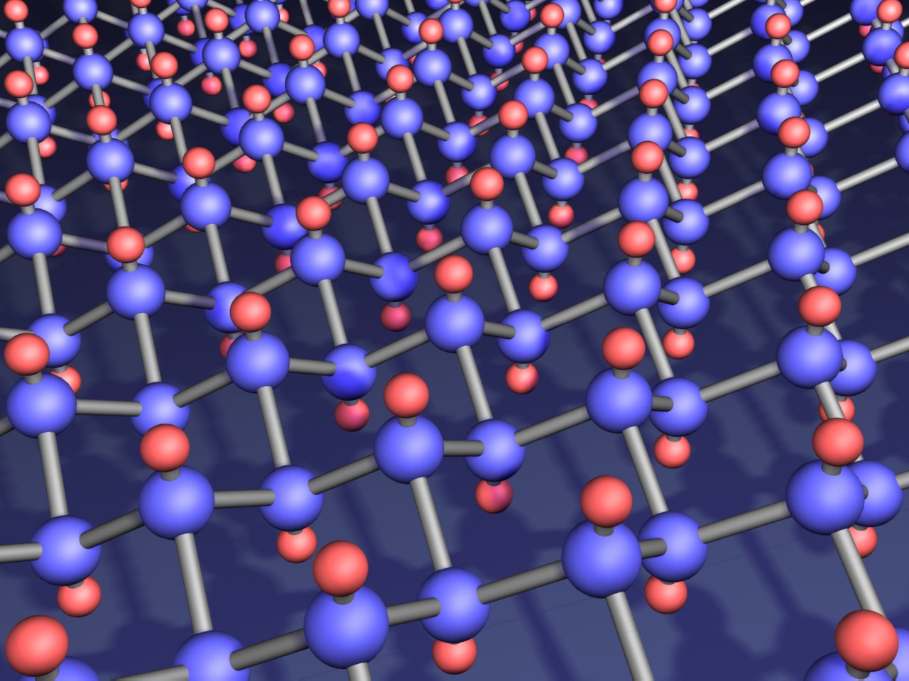
Artistic impression of Hofstadter butterfly effect in graphene/BN heterostructures exposed to mangetic field. In such heterostructures Moire pattern arises due to mismatch and rotation between atomic lattices of graphene and hexagonal boron nitride. PDF file.
Please, acknowledge Columbia University in case you are planning to use this image.
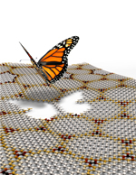
Artistic impression of Hofstadter butterfly effect in graphene/BN heterostructures exposed to mangetic field. In such heterostructures Moire pattern arises due to mismatch and rotation between atomic lattices of graphene and hexagonal boron nitride. TIFF files.
Please, acknowledge Columbia University in case you are planning to use these images.
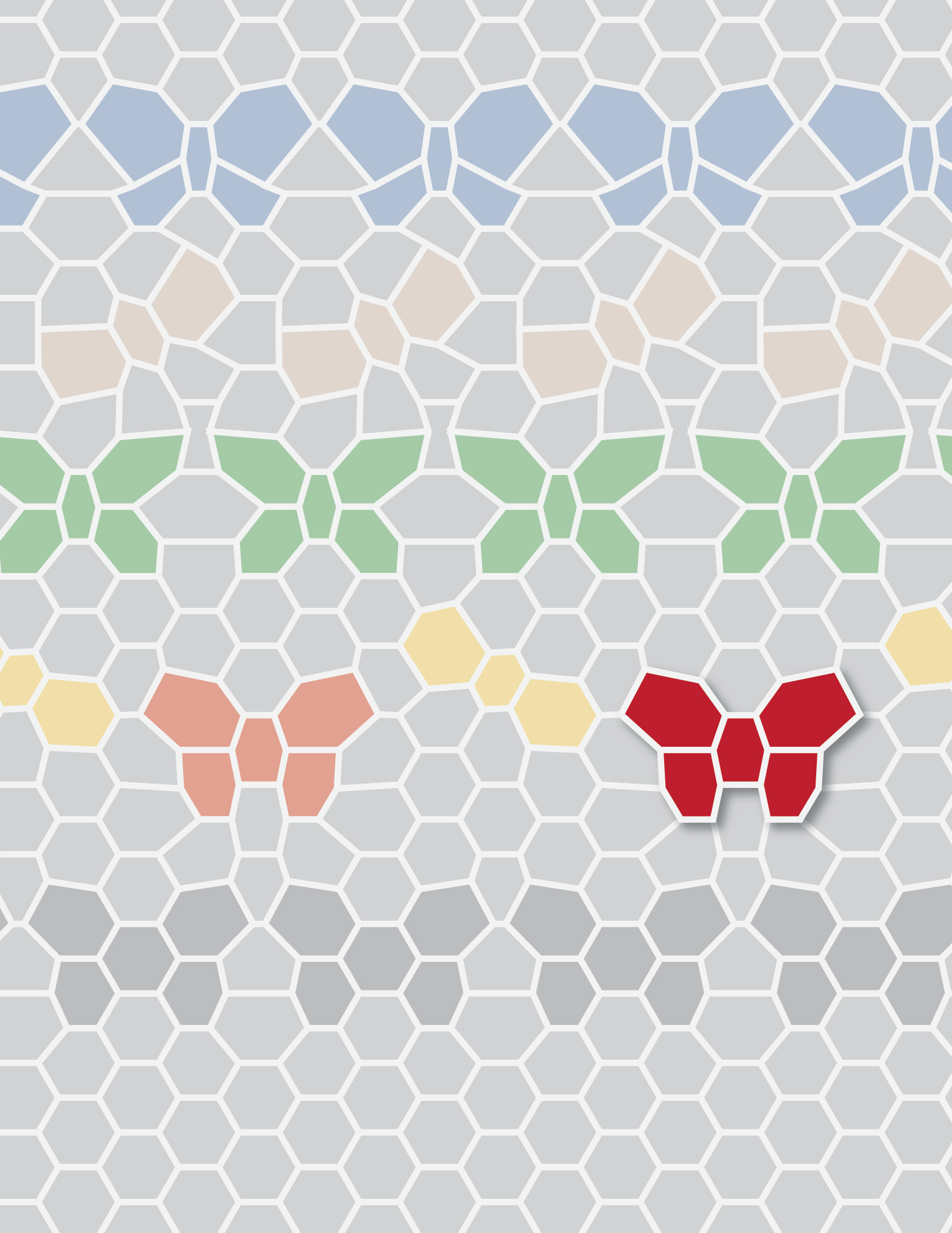

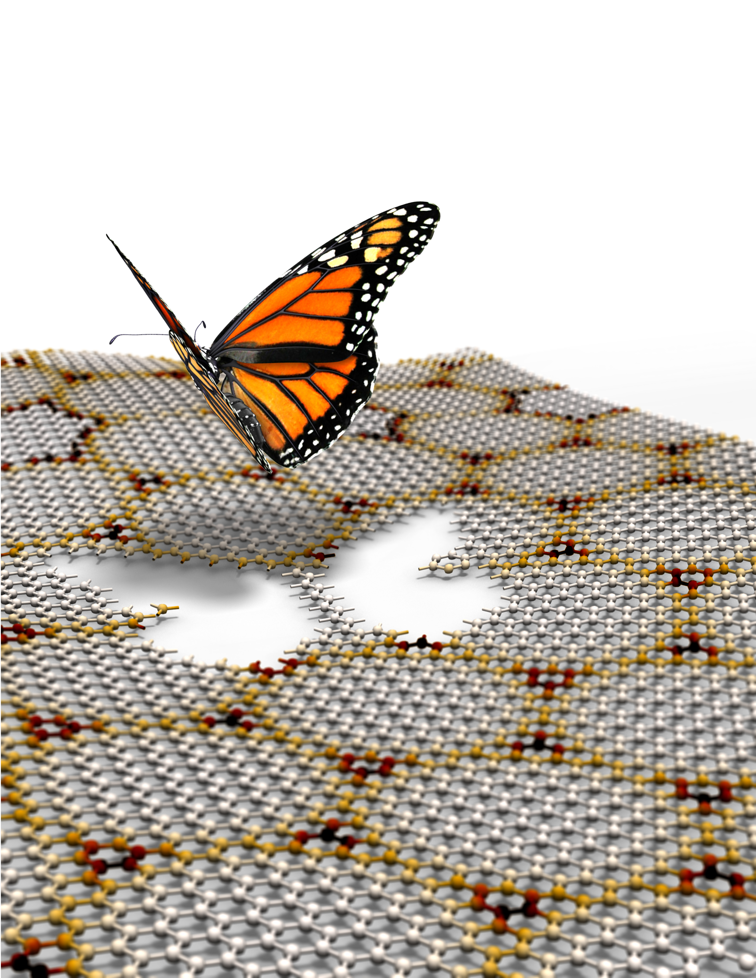
Artistic impressions of Hofstadter butterfly effect in graphene/BN heterostructures exposed to mangetic field. In such heterostructures Moire pattern arises due to mismatch and rotation between atomic lattices of graphene and hexagonal boron nitride. JPG files.
Please, acknowledge Columbia University in case you are planning to use these images.


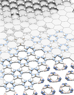
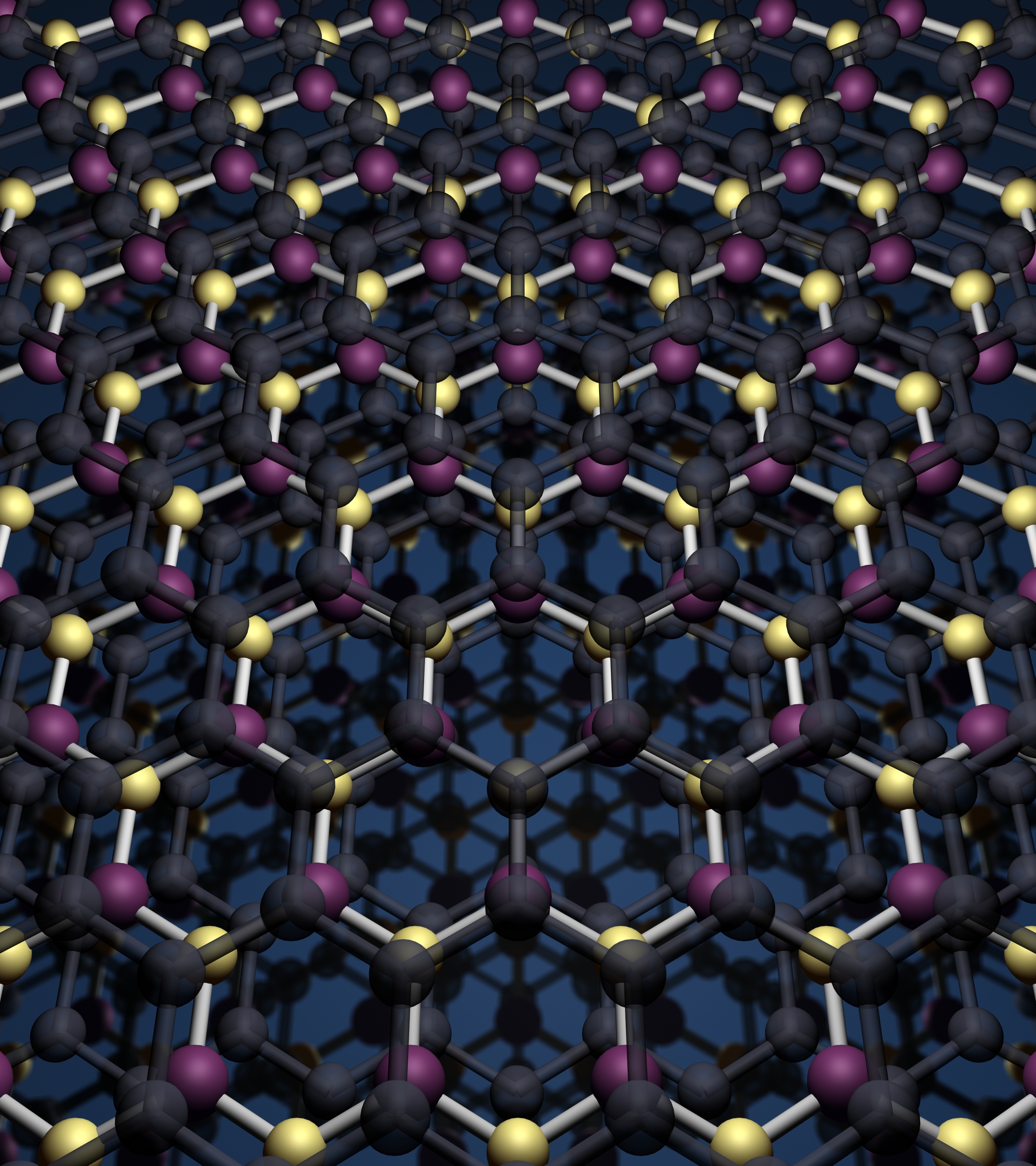
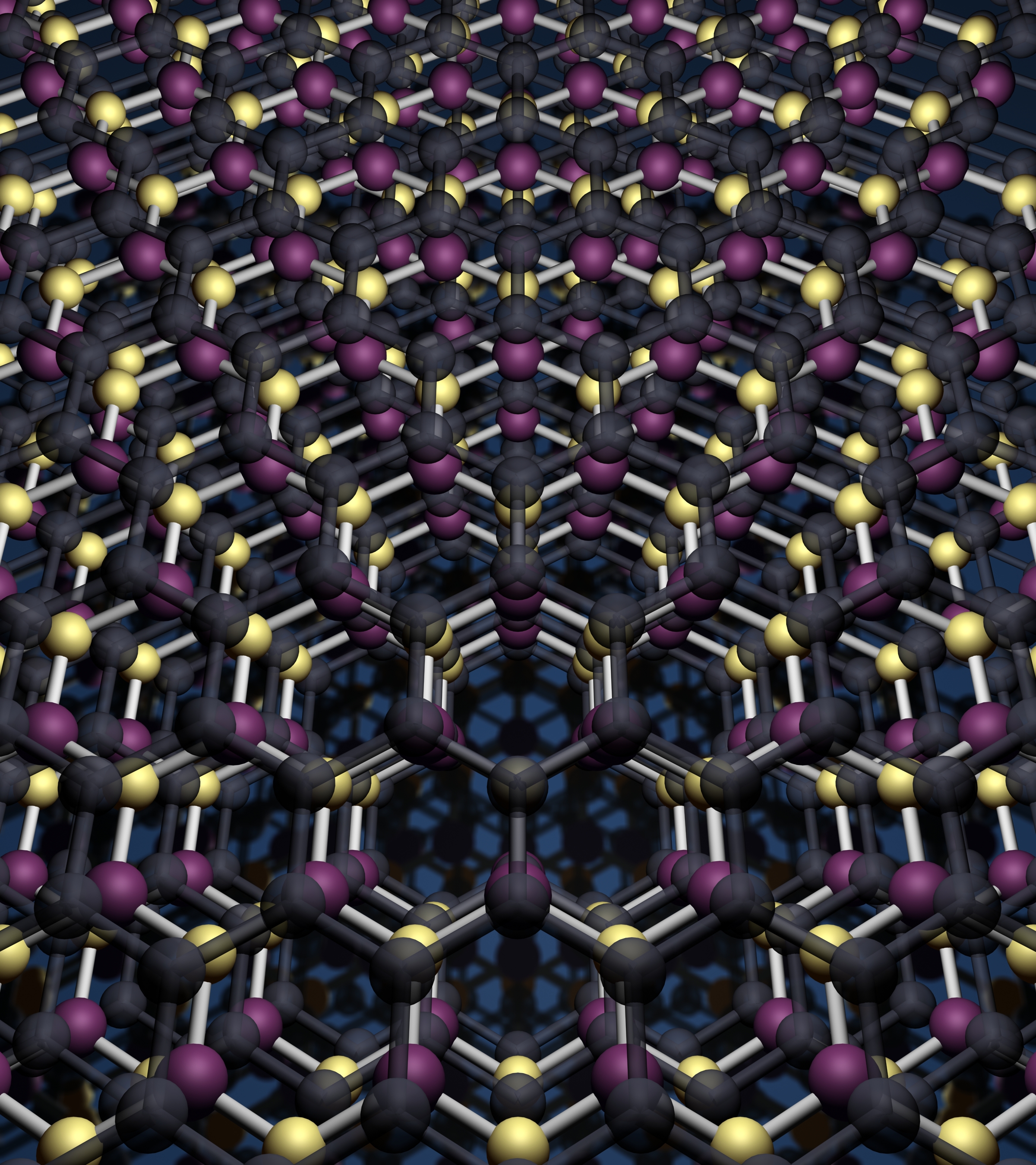
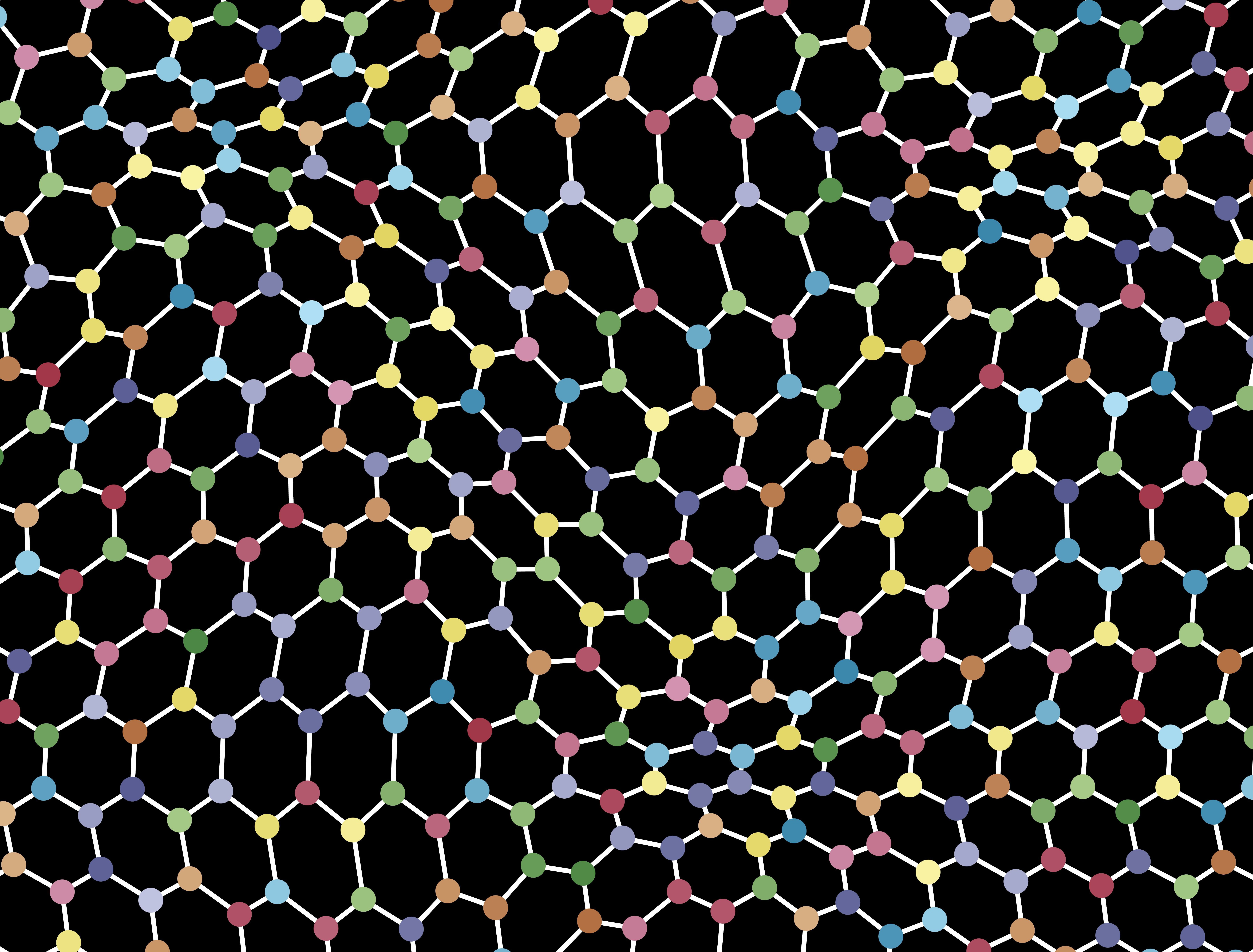
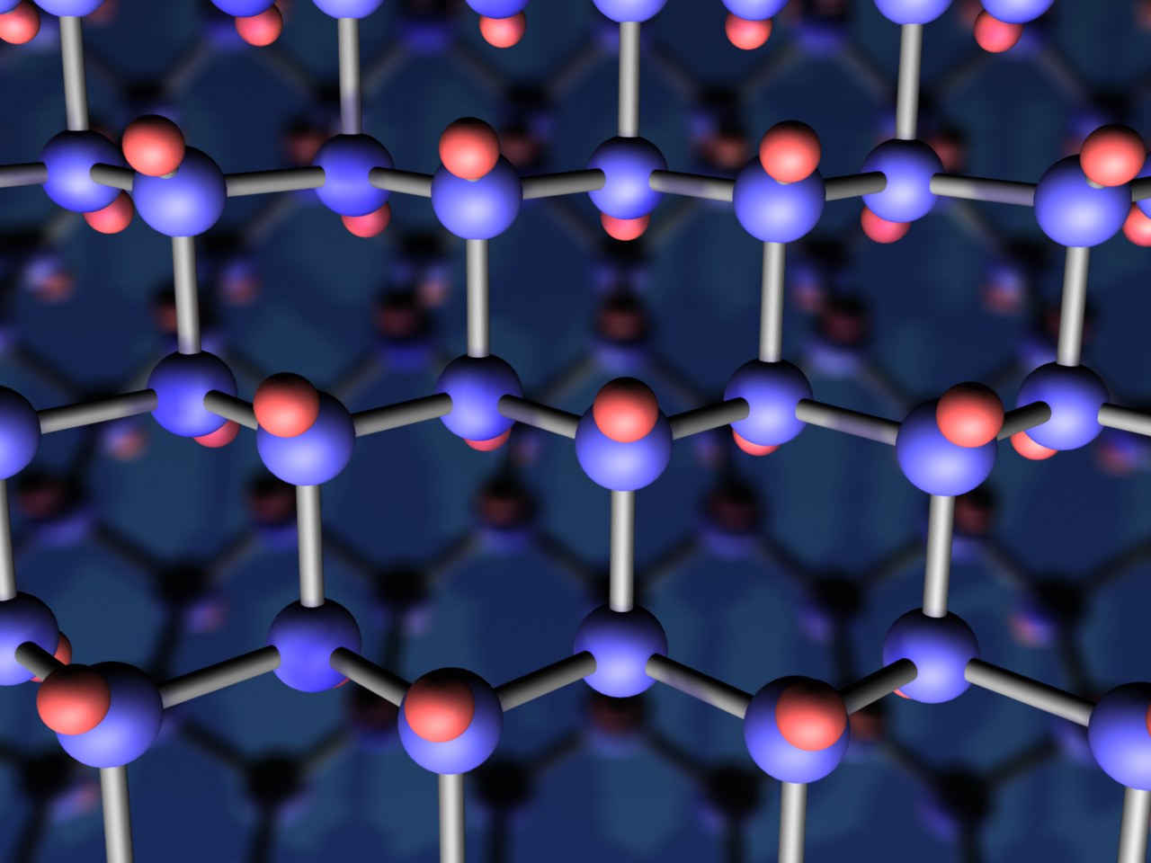
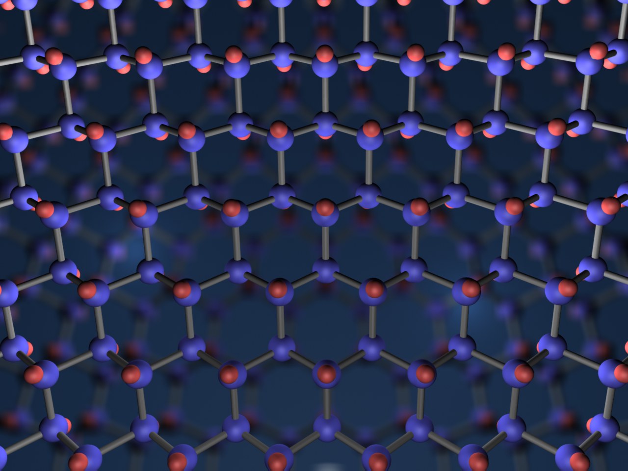
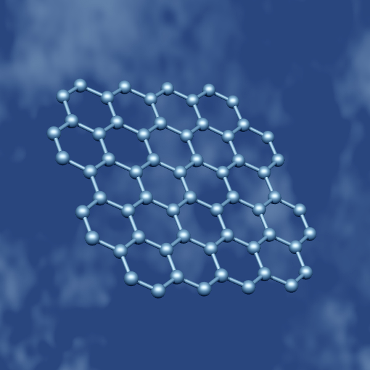
Moire pattern due to mismatch and rotation between atomic lattices of graphene and hexagonal boron nitride
Heterostructures based on 2D atomic crystals for photovoltaic applications
Landau fan-diagram for a high-quality graphene capacitor
![]()
![]()
Tunnelling transistor based on vertical graphene heterostructures. Tunnelling current between two graphene layers can be controlled by gating
Graphene/Boron Nitride heterostructure - Dr Kostya Novoselov
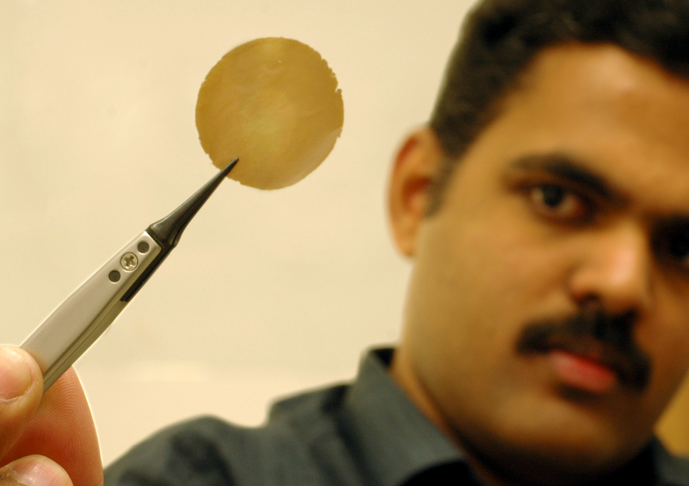
Dr. Rahul R. Nair (who carried out this work) shows his research sample: one micron thick graphene oxide film.
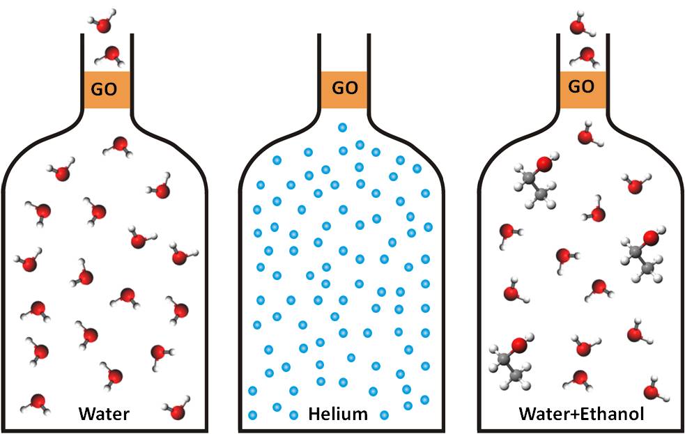
Artistic view:Water easily evaporates through graphene oxide membranes but they represent an impermeable barrier for other molecules - Dr Rahul R.Nair
Interaction-driven spectrum reconstruction in bilayer graphene.
Artistic impressions of the Dirac cones reshaped by e-e interaction by Prof. Kostya Novoselov and Dr Daniel Elias.
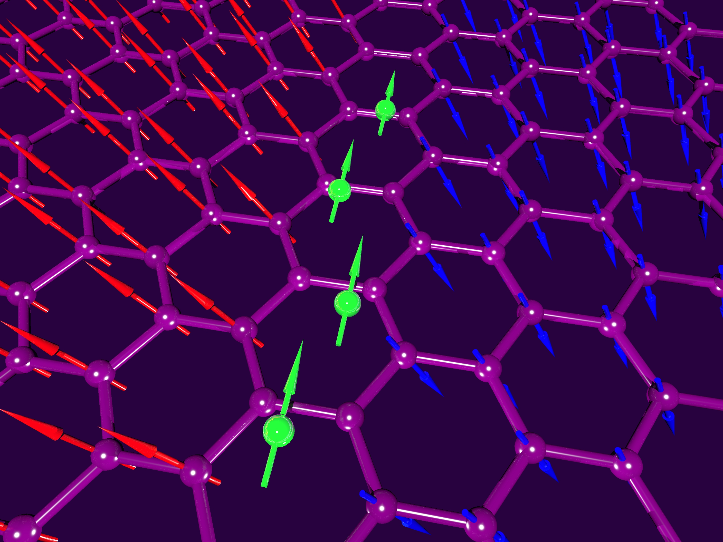
Zeeman-induced spin Hall effect in graphene by Dr Daniel Elias.

Strain in graphene opens up a pseudomagnetic gap.

Graphane crystal. This novel two-dimensional material is obtained from graphene (a monolayer of carbon atoms) by attaching hydrogen atoms (red) to each carbon atoms (blue) in the crystal.
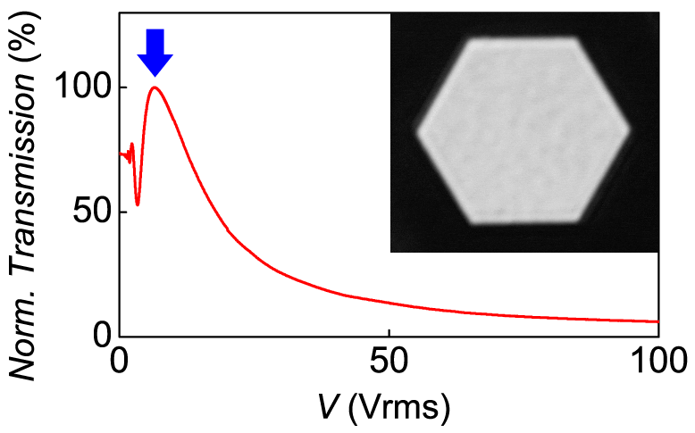
Liquid Crystal Device with electrodes made of graphene with different voltages applied. The overall width of the image is 30 microns.
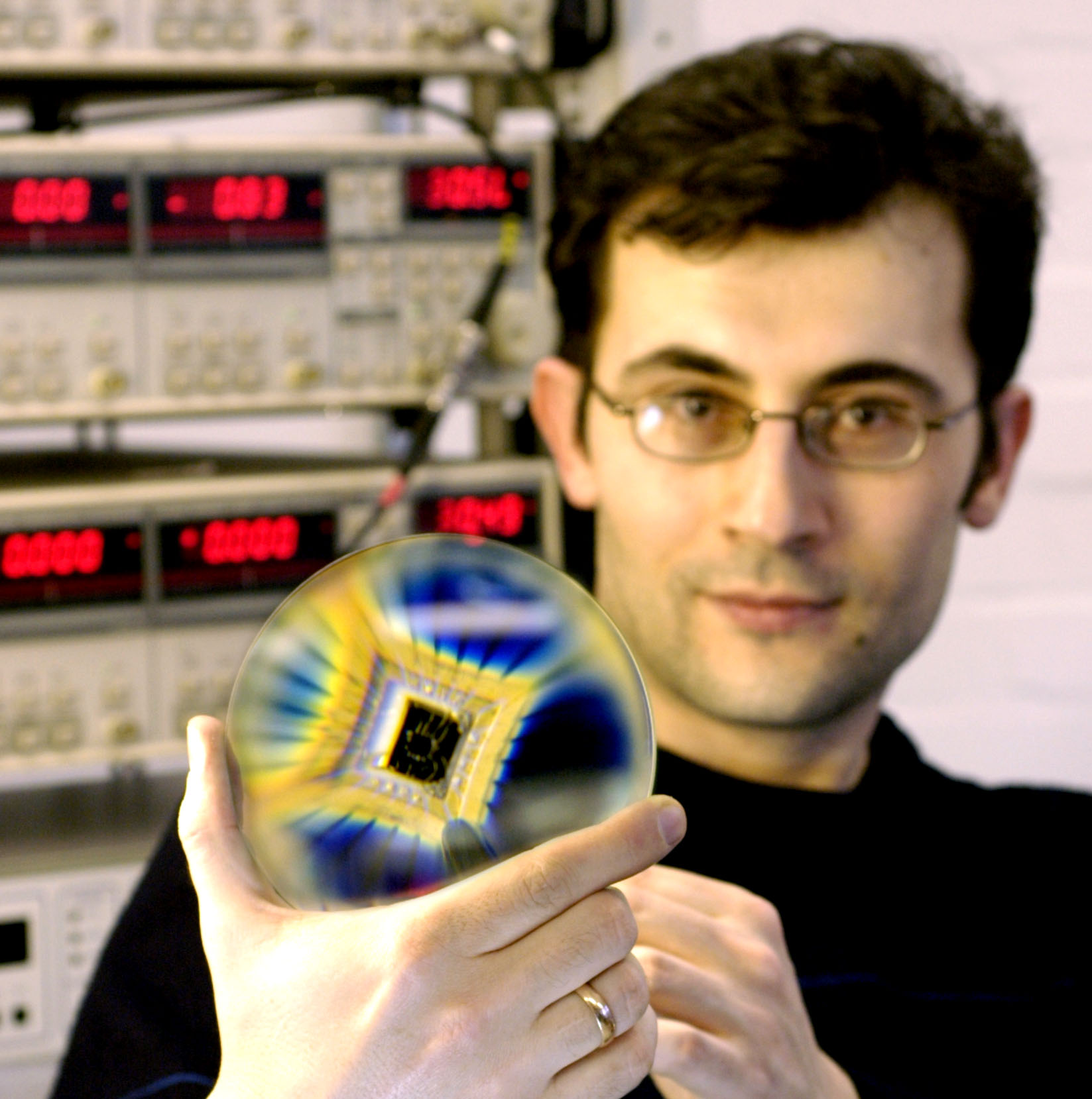
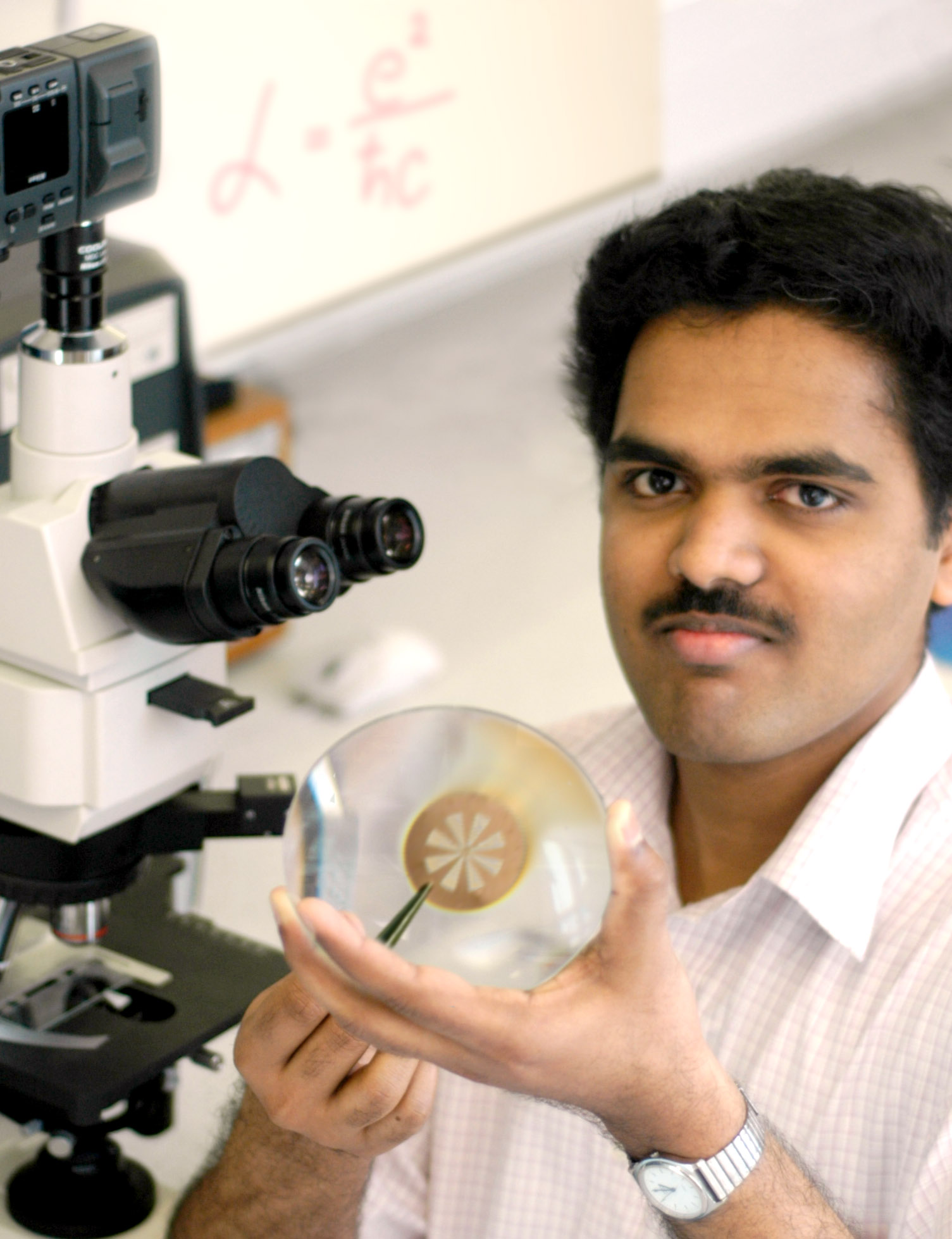
Dr Ponomarenko (who carried out this work) shows his research sample: graphene quantum dots on a chip.
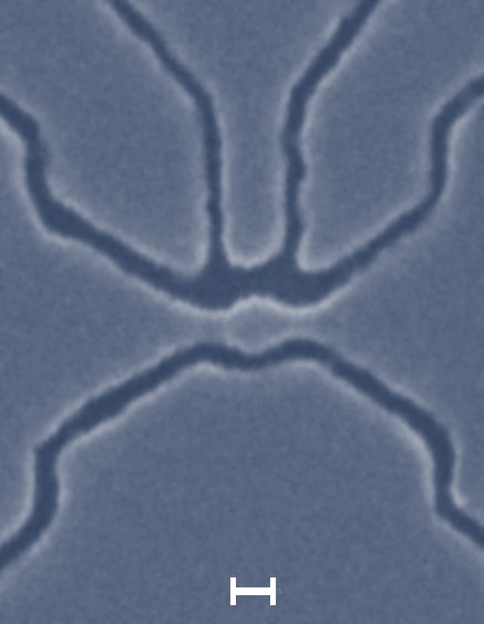
SEM image of a graphene quantum dot device. The scale bar is 20 nm.
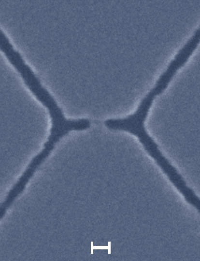
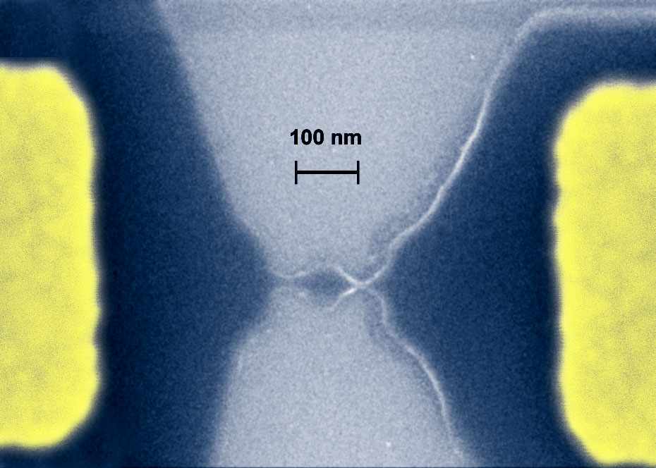
SEM image of a nanoconstriction in graphene. The scale bar is 20 nm.
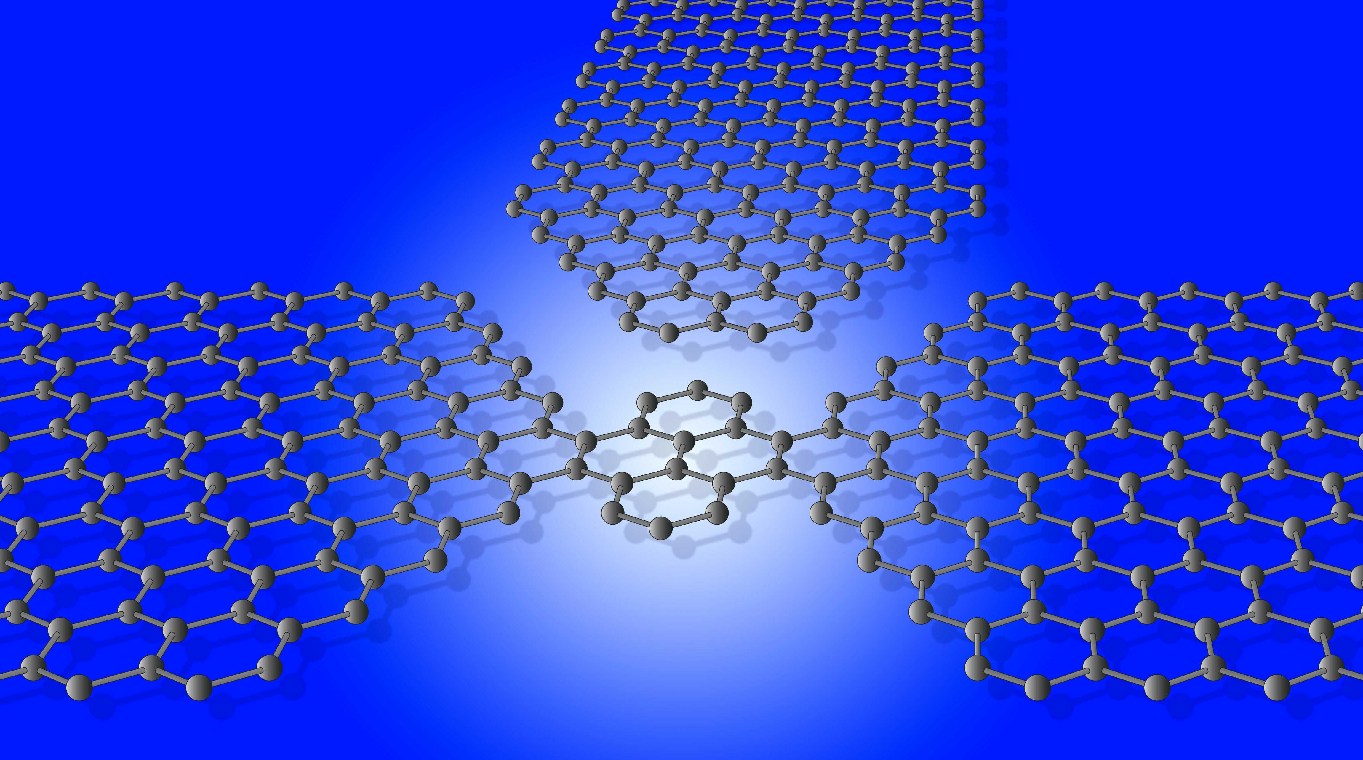
Artistic view of our smallest (nanometre size) quantum dot.
PhD student Rahul Nair (who carried out this work) shows his research sample: a scaffold in which several apertures are covered by graphene.
Magnified image of research samples with small holes covered by one-atom-thick graphene. One can see light passing through them by the naked eye.
The fine structure constant makes graphene visible. Looking through an aperture partially covered by graphene (central stripe) and two layers of graphene (region to the right), one can directly compare their opacities. The central region absorbs 2.3 percent of incident light and the bilayer region twice more.
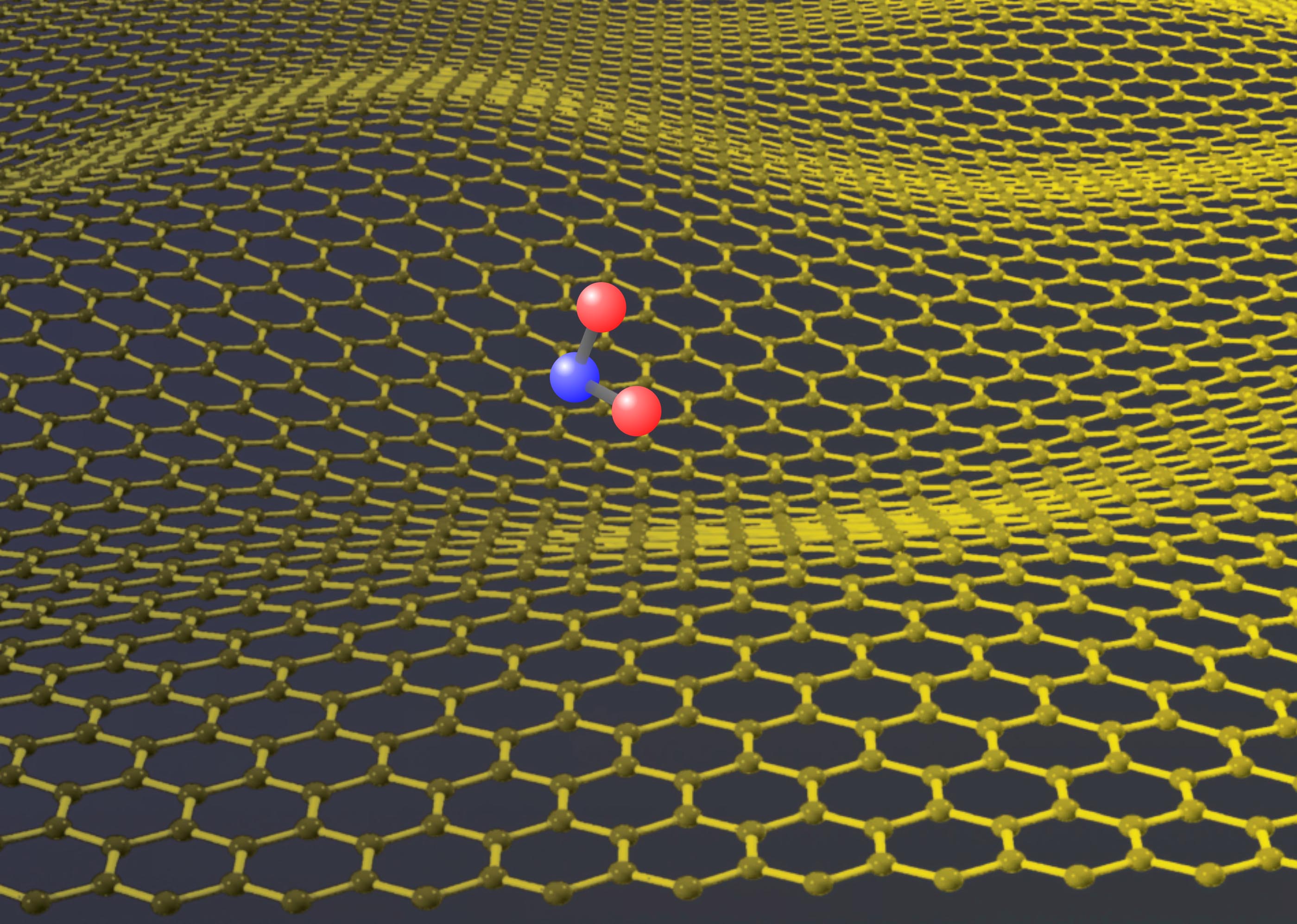
NO2 molecule on graphene surface
Quantum dot carved from a graphene sheet.

Bright-field TEM image of a suspended graphene membrane. Its central part (bluish) is monolayer graphene. Electron diffraction images from different areas of the flake show that it is a single crystal without domains. We note scrolled top and bottom edges and a strongly folded region on the right. The typical distance between the golden bars is 500 nm. Credit to Jannik Meyer
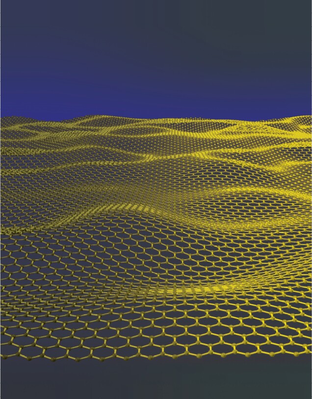
Artistic impression of a corrugated graphene sheet. JPG file (160 Kb). Credit to Jannik Meyer
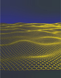
Artistic impression of a corrugated graphene sheet. PDF file (4 Mb). Credit to Jannik Meyer
![]()
Artistic impression of a corrugated graphene sheet. No Background. JPG file (30 Mb). Credit to Jannik Meyer

Artistic impression of a corrugated graphene sheet. No Background. PNG file (30 Mb). Credit to Jannik Meyer

Artistic impression of a corrugated graphene sheet. No Background. JPG file (28 Mb). Credit to Jannik Meyer

AFM image of a graphene molecule. The window size is 10x10 micron (the graphene film is only one atom thick but approx. 100,000 atoms long in the two lateral directions (i.e. contains many billions of carbon atoms).
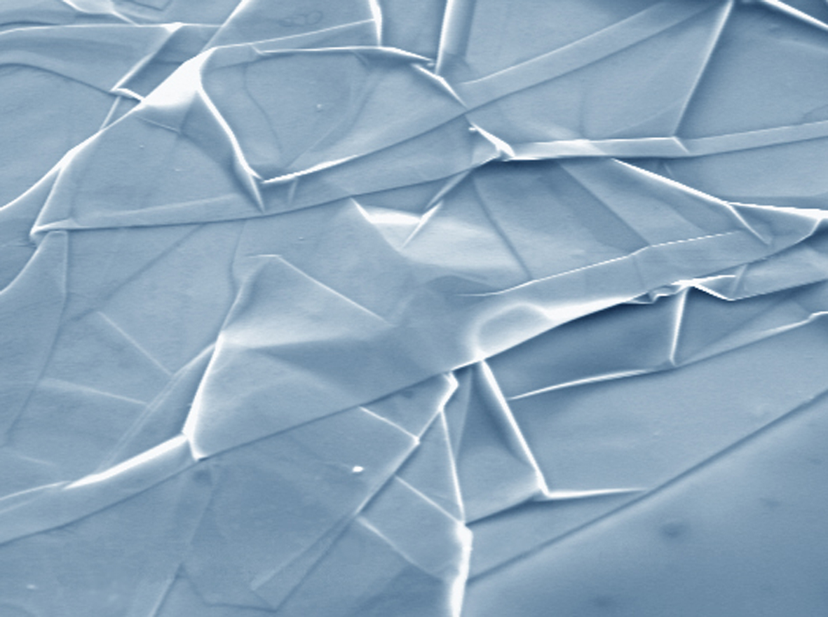
Graphene nanofabric. SEM micrograph of a strongly crumpled graphene sheet on a Si wafer. Note that it looks just like silk thrown over a surface. Lateral size of the image is 20 microns. Si wafer is at the bottom-right corner.
Artistic impression of graphene molecules. Samples of carbon "nanofabric" studied in the Science report are much much larger laterally: they consist of many billions of carbon atoms but still only a single atom thick.
Image "graphene molecule.jpg" is copyrights of Chris Ewels (www.ewels.info)

Scanning electron micrograph (in false colour) of a transistor made on a part of single-layer graphene. Au contacts are shown in gold, SiO2/Si substrate is blue. The width of the graphene wire is 200 nm.
Graphene flakes of different thickness (1, 2, 3, 4 and more layers). Optical photo in normal white light. Lateral size of the image is 200 microns.

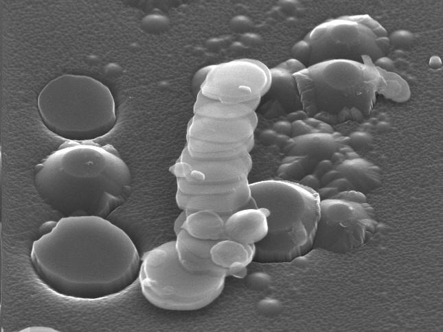
Scanning electron micrograph of a fallen mesa of graphite. This is the way graphene molecules were "extracted" from bulk graphite. To be reasonably visible in SEM, we show a 10 nm carbon flake (30 layer thick).
AFM image (3x3 micron in size) of single-atom-thin carbon nanofabric. Notice that graphene looks just like a silk tissue thrown on a surface: it is creased with many folds, pleats and wrinkles.

Researchers use electron-beam lithography to microfabricate graphene devices
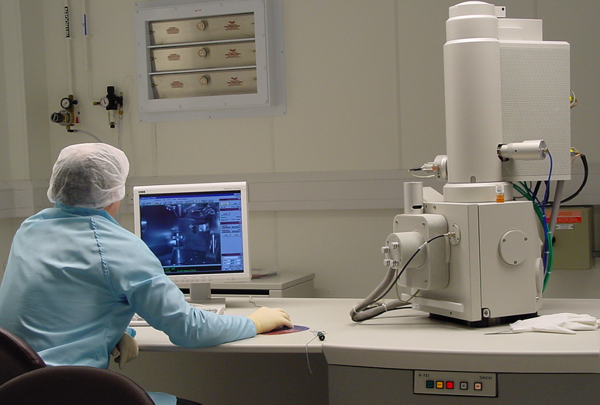
Dr Irina Grigorieva behind our SEM before looking at the prepared graphene devices.